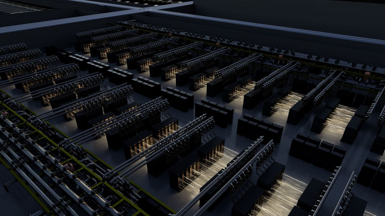
Nvidia used its Hot Chips presentation on the Rubin GPU to argue that facility power, not chip performance, is the real ceiling on AI data centers. The company detailed its DSX MaxLPS (Land, Power, Shell) toolkit, which replaces static, worst-case power provisioning with dynamic, chip-to-rack-level monitoring that reallocates unused power to busier systems. Nvidia says the approach, combined with Rubin's support for 45°C liquid coolant inlet temperatures, lets operators fit roughly 40,000 Rubin GPUs into a 100MW budget for an estimated 2 zettaFLOPS of NVFP4 inference performance; the company has verified similar benefits on current Grace Blackwell GB300 systems, where MaxLPS cut typical GPU power from an assumed 1400W to 1000W without hurting delivered performance. Nvidia acknowledged its Rubin-generation figures are projections rather than measured results.
Several presenters focused on new CPU and memory architectures built around power efficiency and capacity rather than peak core count. Fujitsu detailed its 144-core Monaka server CPU, which splits compute (on a 2nm TSMC die), cache (on a separate 5nm SRAM die holding the entire last-level cache), and I/O across three stacked dies, and narrows its vector units from the 512-bit SVE of its A64FX predecessor to 256-bit SVE2 to reduce core size. Fujitsu says ultra-low-voltage operation lets it pack 144 cores into a 350W or 500W envelope and claims up to double AI performance and over 50% TCO reduction versus unnamed rivals, though these figures remain company estimates ahead of a 2027 launch. Separately, Arm disclosed detailed specifications for its AGI data-center CPU, a dual-chiplet design with up to 136 Neoverse V3 cores, 12-channel DDR5-8800 memory support, and a 2 TB/s UCIe link between chiplets; unlike AMD, Intel, and Nvidia, Arm keeps compute and I/O on the same die per chiplet, a choice aimed at maximizing memory bandwidth and low latency rather than modularity. Arm's only public performance claim so far is a 2x per-rack performance estimate versus current x86 platforms, without conventional benchmark data.
Memory capacity and bandwidth trade-offs were a recurring theme. d-Matrix presented Raptor, which it calls the first 3D DRAM accelerator for generative inference, stacking a TSMC 4nm compute die directly on a custom DRAM die for a claimed 100 TB/s of bandwidth from 32GB per card, with per-card projections such as 988 tokens per second on a 2.8-trillion-parameter model. However, d-Matrix has not disclosed who manufactures its custom DRAM die, and all performance figures are projections from early silicon and simulation rather than third-party-verified results; the company also acknowledged its DRAM density is roughly half that of HBM4 because it isn't using a leading-edge memory process.
Samsung and XCENA both pursued in- or near-memory computing to ease bandwidth and cost pressure. Samsung introduced LPDDR5X-PIM, which adds processing logic directly into each memory bank of LPDDR5X, claiming an eightfold bandwidth increase (to 614 GB/s) and preliminary results showing 2.28x faster model run time and 3.01x higher tokens-per-second in an edge AI inference test versus standard LPDDR5X, without an expected increase in overall power draw despite higher peak power bursts. XCENA presented MX1, a CXL Type 3 memory device combining up to 2TB of DDR5 expansion, SSD-backed capacity, and more than 1,000 RISC-V cores for near-memory computing, reporting up to 4.7x higher throughput and 18.7x greater energy efficiency than a host CPU processing data over CXL on select data-processing workloads; XCENA plans mass production by the end of 2026.
OXMIQ Labs offered a more cautionary assessment of High Bandwidth Flash (HBF), a NAND-based memory format proposed as a lower-cost alternative to HBM. OXMIQ's modeling found HBF can deliver up to 14 times more memory capacity than HBM at similar cost but only about 60% of the aggregate bandwidth, making it best suited to niche cases such as storing mixture-of-experts weights, long-context KV caches, or fitting huge models onto fewer GPUs — not as a general HBM replacement. The company concluded that HBM remains preferable for maximizing throughput across a fully utilized rack, summarizing its view as 'HBM for the rack, HBF for the box,' while also noting that using HBF in practice would require substantial software changes across inference frameworks and accelerator vendors.
Taken together, the Hot Chips 2026 presentations show a shared industry focus on power management and memory architecture as the primary levers left for improving AI system economics, with vendors diverging on strategy: Nvidia and Arm emphasize dynamic power and bandwidth-optimized CPU design, Fujitsu and d-Matrix pursue novel die-stacking for efficiency and bandwidth, and Samsung, XCENA, and OXMIQ explore new memory tiers to address capacity and cost. Most of the performance and efficiency claims discussed, across nearly every company, remain vendor estimates or early-silicon projections rather than independently verified results.