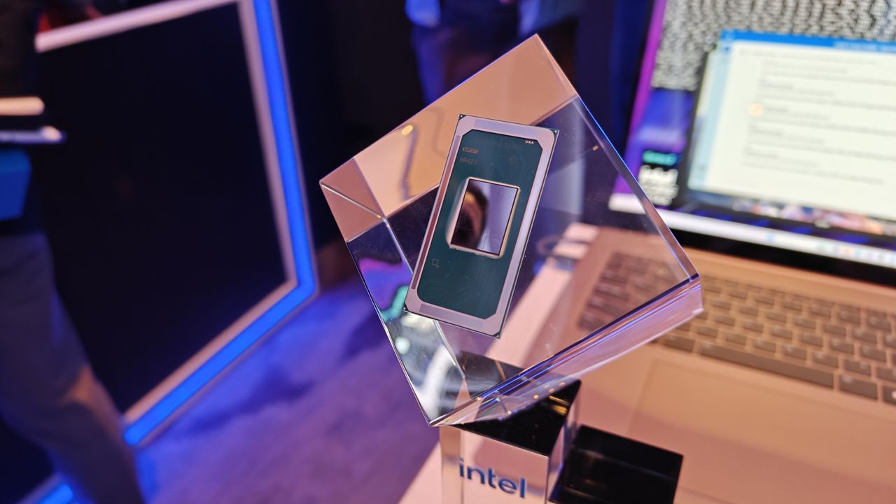
Intel used its Hot Chips 2026 presentation to explain the engineering behind Wildcat Lake, the entry-level 'Core Series 3' chip family for budget laptops. Lead engineer Lance Hacking said Intel faced a choice between a monolithic design or a basic Multi-Chip Package (MCP), since its advanced Foveros 2.5D/3D packaging was too costly for a budget part. Instead, Intel adopted the Universal Chiplet Interconnect Express (UCIe) standard, an open interconnect specification that debuted in 2022 around the time Wildcat Lake's planning began.
Unlike typical budget chips that reuse older 'N-1' generation IP, Wildcat Lake pairs Intel's newest 18A process for its compute die with a separate I/O die built on an N6 process node (Tom's Hardware identifies the foundry as ISMC, while Wccftech identifies it as TSMC). Skipping Foveros in favor of MCP eliminated the need for a costly base die, cutting assembly costs and improving yields, but it also required a larger interconnect: Wildcat Lake's UCIe die-to-die interface is 70% larger than the Foveros interconnect used in Intel's higher-end Panther Lake chips, due to a larger bump pitch (110 microns for UCIe versus 36 microns for Foveros). Intel says the added area was worth the overall cost savings.
The switch to UCIe also raised power concerns, particularly since display signals must cross the UCIe link. Intel identified idle power draw without panel self-refresh as the biggest concern and addressed it by adding a buffer to hold panel refresh data before the UCIe connection. Separately, Intel capped the UCIe transfer rate at 8 GT/s, well below the 64 GT/s the UCIe 3.0 specification allows, which still supports PCIe 4 SSDs and 4K60 external displays while reducing bit-rate errors and letting Intel remove some error-correction circuitry.
To make room for UCIe and control costs, Intel trimmed both dies substantially. The compute die drops to two Xe graphics cores (from four) without a dedicated ray-tracing accelerator, reduces the NPU from three tiles to one, and moves to a narrower 64-bit memory bus with lower speeds and capacity. Wccftech reports the NPU delivers 17 TOPS (40 platform TOPS total), cache is reduced (6MB LLC versus 12MB, and a 2MB system cache versus 4MB), and P-cores are limited to two. Display support drops to three pipelines instead of four; Tom's Hardware reports Intel used HBR3 rather than UHBR20 bandwidth, while Wccftech states the chip retains UHBR20 support. These cuts reduced the compute die's size by 38%. The I/O die lost its camera PHY entirely, along with reduced PCIe/USB lane counts and a slimmed-down audio engine, for a 15% reduction in die area.
Beyond the silicon, Intel pursued broader bill-of-materials savings under its 'Project Firefly' initiative, which leverages the mobile supply chain for budget laptops. These include integrating Wi-Fi 7 and a USB power-delivery controller directly into the chip, and using a 6-layer PCB instead of eight layers thanks to the simpler memory bus. Intel also added a dedicated power rail for its low-power efficiency (LPE) core cluster—an added cost, but one intended to let lightweight workloads run on the LPE cluster and preserve battery life, given that most Wildcat Lake SKUs include only one or two performance cores. When binning chips into different SKUs, Intel recovered partially defective dies for compute components like P-cores, Xe cores, and NPUs, but did not attempt recovery on LPE clusters, display pipelines, or I/O, since Intel considered those critical to maintaining consistent battery life and platform behavior across the lineup.
Both outlets frame Wildcat Lake as an unusual departure from typical budget chip design, since it applies Intel's latest and most expensive process technology to an entry-level product rather than repurposing older silicon. Tom's Hardware notes that competitors like the MacBook Neo and Snapdragon C rely on more traditional 'N-1' chip designs for their budget offerings, and reports that Wildcat Lake won a Tom's Hardware innovation award for 2026. Wccftech adds that Wildcat Lake's smaller MCP package (35x25x1.23mm) is notably more compact than the Panther Lake package (50x25x1.5mm), contributing to further board-space and cost savings.