SanDisk and SK hynix have formally released the High Bandwidth Flash (HBF) specification through the Open Compute Project (OCP), making it an open standard rather than a proprietary interface. The release comes roughly six months after the OCP consortium's HBF workstream began in February, with SanDisk and SK hynix serving as primary contributors. Google and Tenstorrent joined as consortium members during the standardization process, while companies including AMD, Broadcom, Intel, Nvidia, Marvell, Micron, Qualcomm, Samsung, and Western Digital have so far not expressed interest in HBF.
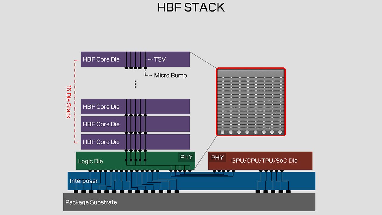
HBF is designed to combine the non-volatility and capacity of 3D NAND with performance closer to High Bandwidth Memory (HBM), creating a new memory tier positioned between HBM and enterprise SSDs. Rather than replacing HBM, HBF is meant to complement it: HBM handles data immediately required for computing, while HBF stores larger volumes of data, such as AI models, at greater capacity. The specification supports packages of up to 512GB using 8-Hi or 16-Hi stacked NAND die configurations, which are specialized devices with a fast interface rather than standard 3D NAND stacks.
Performance is divided into three bandwidth grades ranging from about 0.4 TB/s to 3.0 TB/s, though it is unclear whether the top figure describes a full HBF subsystem or a single package. The highest bandwidth tier would exceed the 2 TB/s bandwidth of a single HBM4 stack, though HBF is expected to trail HBM4 in latency. Achieving over 400 GB/s from a single 512GB package could involve using many core dies with concurrent read/write paths, or a single UCIe interface running at up to 64 GT/s across 64 lanes, which would require a fairly complex base die.
HBF is described as using the Universal Chiplet Interconnect Express (UCIe) standard to simplify integration with heterogeneous computing platforms. SanDisk refers to its host interface as 'xPU-HBF,' which may represent its implementation of UCIe as adopted by companies like Broadcom or Marvell. The specification also defines electrical and interface characteristics, packaging and reliability guidelines, and software I/O requirements for read and write operations, though the full technical documents have not yet been officially published by OCP.
SK hynix's Kim Chun-sung, head of solution development, said the company aims to expand the boundaries between memory and storage to build new architectures that improve system efficiency. SanDisk's chief technology officer, Alper Ilkbahar, said the specification gives system designers a practical path to bring high-capacity, high-bandwidth memory closer to compute while enabling more flexible architectures. SanDisk and SK hynix plan to discuss HBF further, including a keynote and a panel with Google, at the Future of Memory and Storage Conference in Santa Clara.
Separately, Samsung is pursuing its own approach for AI inference storage needs, developing and mass-producing CMX solutions in collaboration with Nvidia, alongside V10 and V11 NAND flash reaching up to 500 stacked layers aimed at fast data access for AI servers. It remains unclear which approach, HBF or Samsung's alternative, will gain broader industry traction in the coming months.