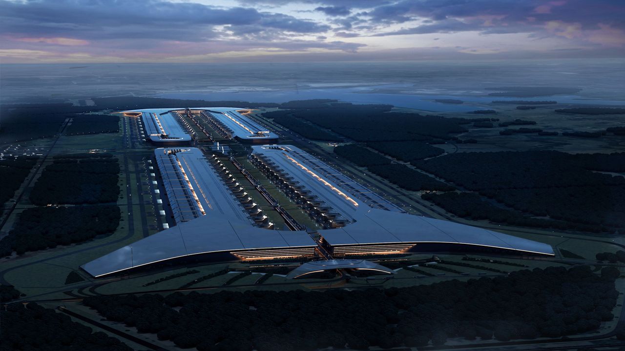
SpaceX and Tesla formally unveiled plans for the initial phase of their joint semiconductor project, known as Terafab, according to Tom's Hardware. The first stage is expected to use Intel's 14A process technology and require $16.8 billion in investment, with the completed campus planned to eventually span more than 100 million square feet of manufacturing space. The facility will be built in Grimes County, Texas, on land belonging to SpaceX.
The companies say their combined demand for semiconductors is projected to exceed 1 terawatt of compute per year, far beyond current global supply, according to Tom's Hardware. SpaceX, Tesla, and xAI already consume a significant share of existing contract chipmaking capacity, and Terafab is envisioned to exclusively produce AI inference processors for Tesla's Optimus humanoid robots and Cybercab autonomous vehicles, as well as high-power processors for SpaceX's space-based data centers. No timeline was given for when demand will reach the 1 TW benchmark.
Terafab is designed as a vertically integrated campus that would house advanced logic devices, memory chips, packaging, and testing operations together, rather than splitting these processes across separate facilities as is standard in the industry, per Tom's Hardware. The companies believe this consolidation will shorten production cycles and speed up yield improvements. Based on images released by SpaceX, the facility will consist of four large buildings, though it remains unclear whether each will handle a different function or represent separate phases of the same integrated process.
The 100-million-square-foot figure is notably larger than any existing semiconductor facility; for comparison, Tom's Hardware noted that Samsung's entire Pyeongtaek campus covers about 31.1 million square feet, with a single fab occupying roughly 1.29 million square feet. The companies clarified that the figure refers to overall manufacturing space rather than cleanroom space specifically. The project is expected to employ at least 3,000 people, with 60% to 80% drawn from Grimes and nearby Brazos County. Terafab will also use water from the Gibbons Creek Reservoir instead of local groundwater, alongside on-site wastewater treatment and water recycling measures. The announcement follows an earlier groundbreaking at Tesla's Giga Texas campus for a research semiconductor facility described as a precursor to Terafab.
Separately, Wccftech reported that Tesla has posted a job listing for a Memory Process Integration Engineer for Terafab, indicating the project is expanding beyond logic chips into memory technology. The role involves driving integration for DRAM cell structures, defining integration schemes for advanced DRAM nodes, and working on emerging memory technologies such as MRAM, RRAM, or 3D DRAM as Terafab's memory roadmap develops. Wccftech noted this suggests Terafab could aim to address the ongoing memory supply crunch that has favored an oligopoly of Samsung, SK hynix, and Micron, though the project remains in its early stages.