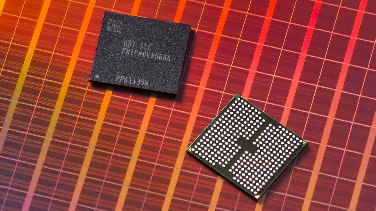
At the Future of Memory and Storage (FMS) 2026 conference, Samsung presented its vision for next-generation memory and storage aimed at AI and general-purpose applications. The company introduced three technologies—zHBM, zNAND-O, and BV-NAND—which target different use cases but all rely on advanced wafer bonding.
zHBM is Samsung's concept for custom high-bandwidth memory that would sit directly on top of an AI accelerator's logic die, rather than beside it as current HBM does. Samsung says this placement shortens the distance data must travel between compute and memory, and projects roughly 8x the performance of HBM5, more than 10x higher memory density, 3x better energy efficiency, and over 50% lower thermal resistance versus HBM5. Tom's Hardware notes these claims are vague, since Samsung does not specify whether 'performance' refers to bandwidth or another combined metric, and HBM5 itself is not yet a finalized standard. Samsung says zHBM will support customer-specific designs and allow custom IP integration between the HBM stack and processor, and is already working with customers on the concept, though no timeframe has been disclosed and it remains in an early concept phase.
zNAND-O is a high-performance NAND technology in development that would place four or eight stacks of NAND atop logic dies, based on Samsung's V-NAND (BV-NAND) platform. It is designed to combine high storage density with improved I/O performance and low latency, and Samsung positions it for edge AI systems handling real-time, data-intensive inference. Samsung has not disclosed detailed schematics or a firm timeline for this technology.
BV-NAND, also called Samsung's 10th Generation V-NAND (V10), is a new brand for the company's next-generation 3D NAND that bonds the NAND array on top of the I/O and logic wafer using hybrid bonding, rather than stacking layers within a single cell. Samsung has said this 400-layer-class NAND reaches an areal density of 28 Gb/mm2 and a maximum I/O speed of up to 5600 MT/s, representing a roughly 58% density increase over its V9 generation along with improved read, write, and I/O performance. Unlike zHBM and zNAND-O, BV-NAND is described as set to reach the market in the near term rather than being years away.
Wccftech reports that Samsung is already planning beyond BV-NAND toward NAND designs exceeding 1,000 layers using hybrid bonding, alongside continued development of memory technologies such as zHBM, HBM4E, HBM5, and GDDR7. Tom's Hardware adds context comparing Samsung's NAND layer counts and density figures to competitors including Kioxia/Sandisk, SK hynix, Micron, and YMTC, noting Samsung's higher I/O speed despite slightly lower density than some rivals' latest NAND generations.
Both outlets agree that zHBM and zNAND-O remain years from commercial availability and are still conceptual, while BV-NAND is closer to real-world deployment. Tom's Hardware suggests the new BV-NAND branding may serve as a marketing tool, since actual SSD performance is often limited by the PCIe interface rather than raw NAND I/O speed, though it notes mid-range PCIe Gen5 SSDs using quad-channel controllers do depend more directly on NAND I/O performance.